Wednesday, June 12, 2013
Night Light Like Mushroom or Clouds
Cute mushroom will illuminate several colors, warm, soft, romantic bright night lights shine in the dark. Five leaves and flowers can be inserted into the grass as long as you like. Light levels will automatically change the brightness according to light elegant warm glow for you to create the most quiet.
Mushroom-shaped styling will take you back to childhood to the recollection of it is joy and childlike. In addition to light according to its role in the day, it also has a decorative function. I believe everyone came to your house of friends, will not help but to touch the cute little house. Such a small lamp, energy saving, up at night when the pat on the light, without headlights.
Reading Cellphones Schematic Diagram
Schematic Diagram is a layout of symbols and and connection of every electronic components circuit where serve as a guide on how the circuit function or work.
Reading Schematic Diagrams is not a hard task to do, schematic diagrams is a big help to cellphone-repair
especially when working on or tracing lines and finding where a particular components mounted on a PCB board.
Such schematic diagrams is very useful and very important guide in every cellphone technician. It is equivalent to a handbook.
Learn how to read it. At first you might think that it is hard to do so, You are not going to be an experts and master in cellphone repair
as long as you don't know how to read it. Many among cellphone
repairman exist nowadays that do not have any knowledge about reading
it. They always rely on finding free solutions over the internet and
forums. Those people who give free solutions are those people who knows
how to read a schematic diagram.
Now here's your chance to learn and do not rely unto others, and be an
expert and master troubleshooter when it comes to hardware problems.
Okay here's a step on how to read a schematic diagrams.
1. You need to download service Schematic Diagrams, as many or complete package in every cellphone products. each unit of a product have specific service diagrams.
2. You need to download Adobe Acrobat Reader so that you can open the schematic file which is in PDF format.
Now assuming that you already have those I've mention above; Let's try
to open up one file like for example we are going to open a schematic diagram of Nokia N70.
here's what it looks like when scrolling down all the pages.
Let's take a little brief on each page for simple understanding..
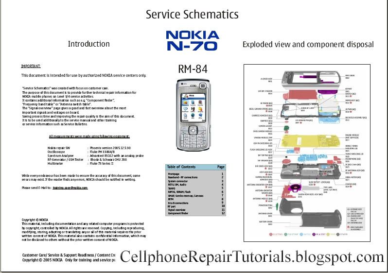
A. page 1, In this page where you can find and Identify the whole assembly of the unit.
this is also where to findd the table of contents of the entire circuit's layouts.
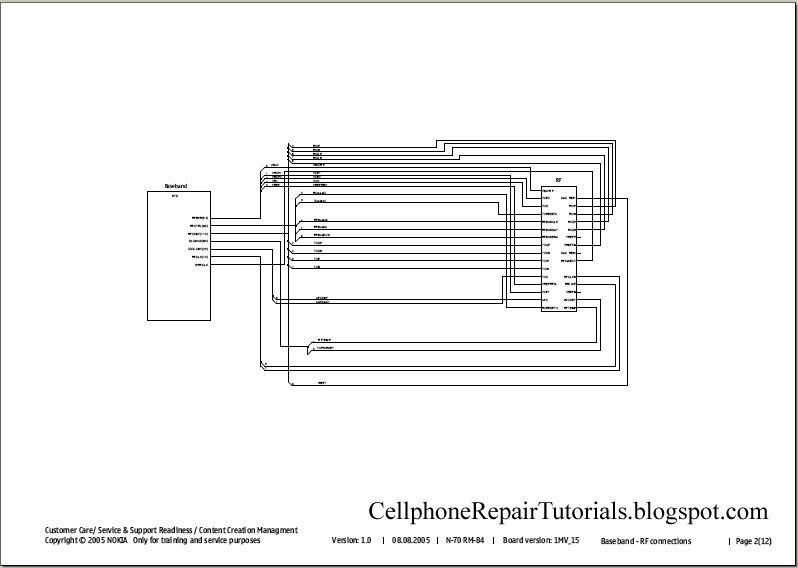
B. page 2, In this page is a block diagram of an RF and Baseband:
this is a basic explanation of the entire connection of a circuit. It
was called a block diagram for it is being drawed into blocks.
What is a BASE BAND?
In telecommunications and signal processing, baseband is an adjective
that describes signals and systems whose range of frequencies is
measured from zero to a maximum bandwidth or highest signal frequency;
it is sometimes used as a noun for a band of frequencies starting at
zero. It can often be considered as synonym to lowpass, and antonym to passband, bandpass or radio frequency (RF) signal.
What is a RF?
Radio frequency (RF) is a frequency or rate of oscillation within the
range of about 3 Hz to 300 GHz. This range corresponds to frequency of
alternating current electrical signals used to produce and detect radio
waves. Since most of this range is beyond the vibration rate that most
mechanical systems can respond to, RF usually refers to oscillations in
electronics circuits.
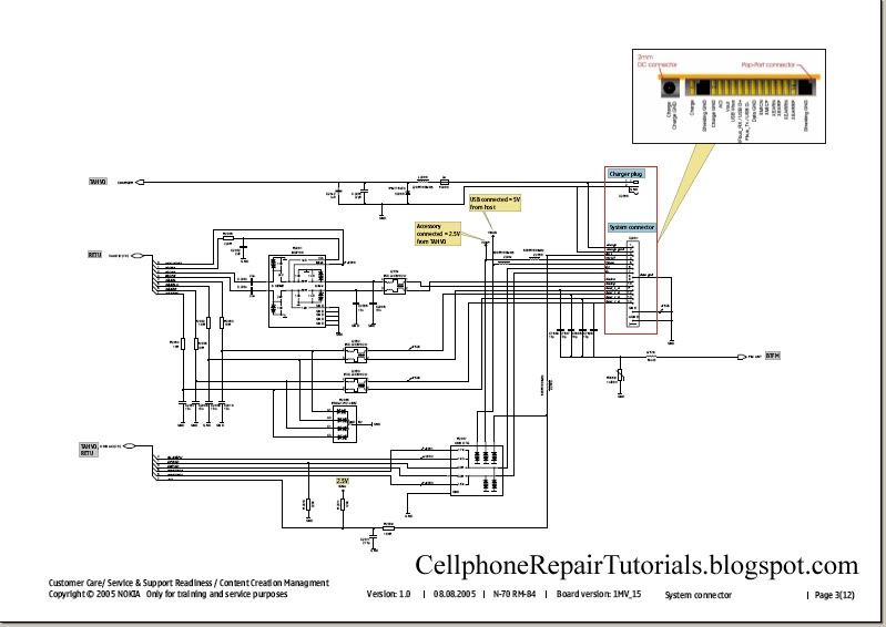
C. page 3, here we can find the system connectors and parts of the unit that correspond to the user or outer parts such us headset, charger and USB connection interfaces.
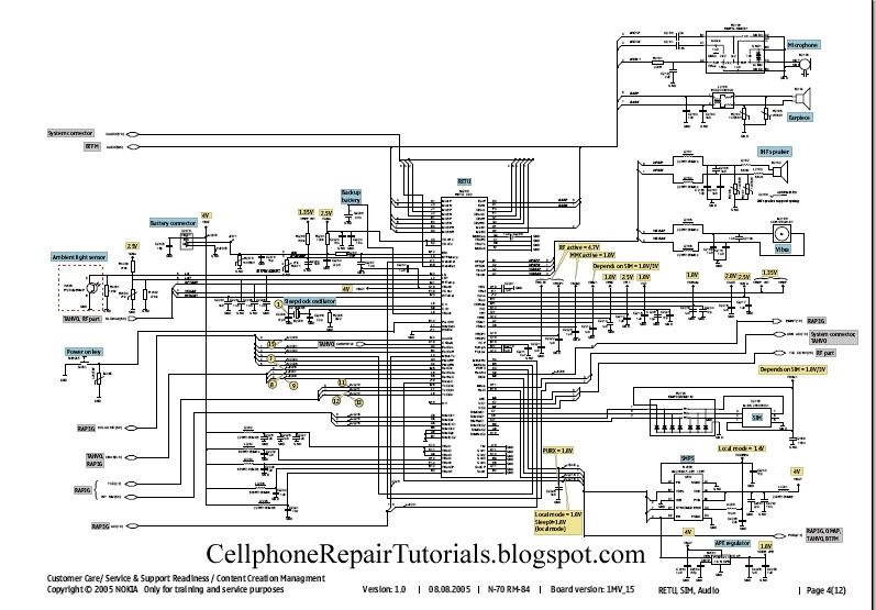
D. page 4, The power management circuit, audio codecs and drivers and the interfaces like the microphone, earpiece, mouthpiece, vibrator, sim-card, battery connections. This is the Power Supply Area of the entire circuits.
E. page5, Charging Control and Flash Interface Circuit.
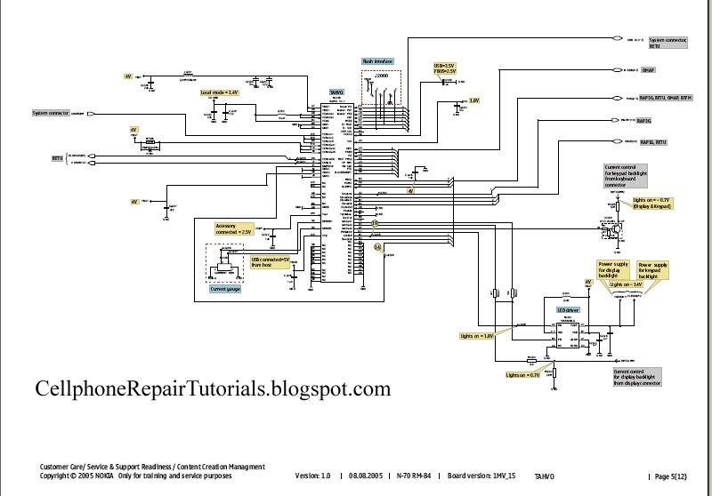
F. page 6, This is the part of the circuit where the all application is being process, Flash IC and memories, this also where application and firmware are being stored.
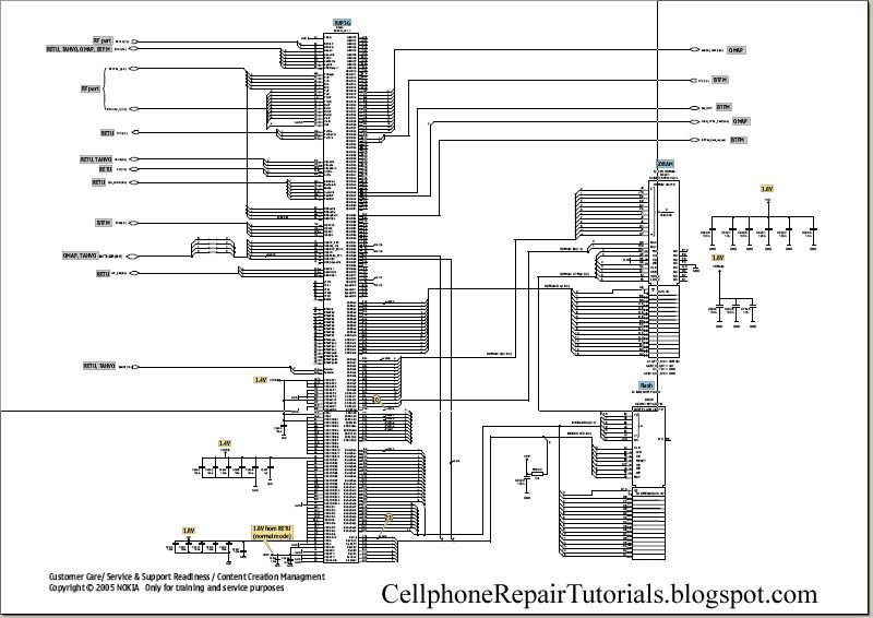
G. page 7, his the Central processing of the unit (CPU) like the personal computer (PC) cellphone also have a CPU to process applications and software.
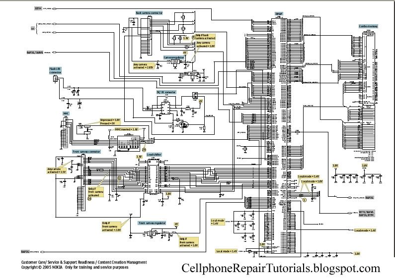
H. page 8, A Frequency Modulation (FM Radio) circuit.
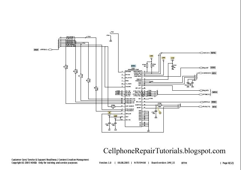
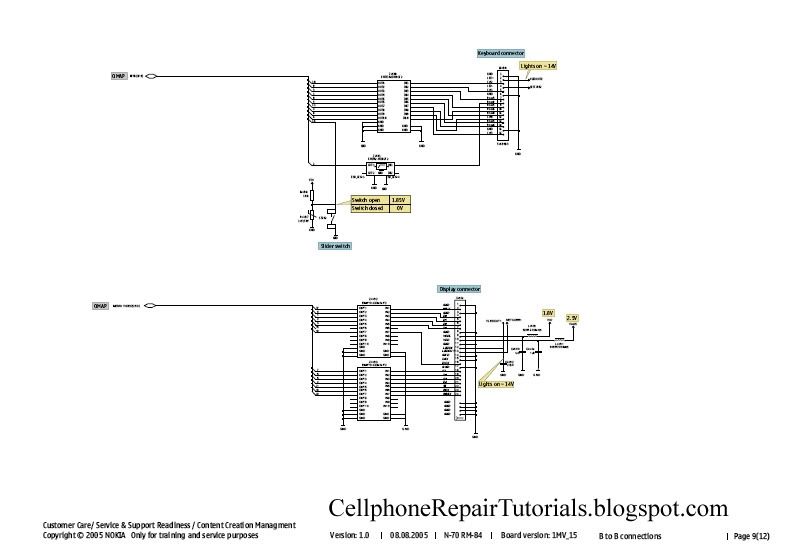
I. page 9,This page is the part of an LCD Display and Keypad circuit.
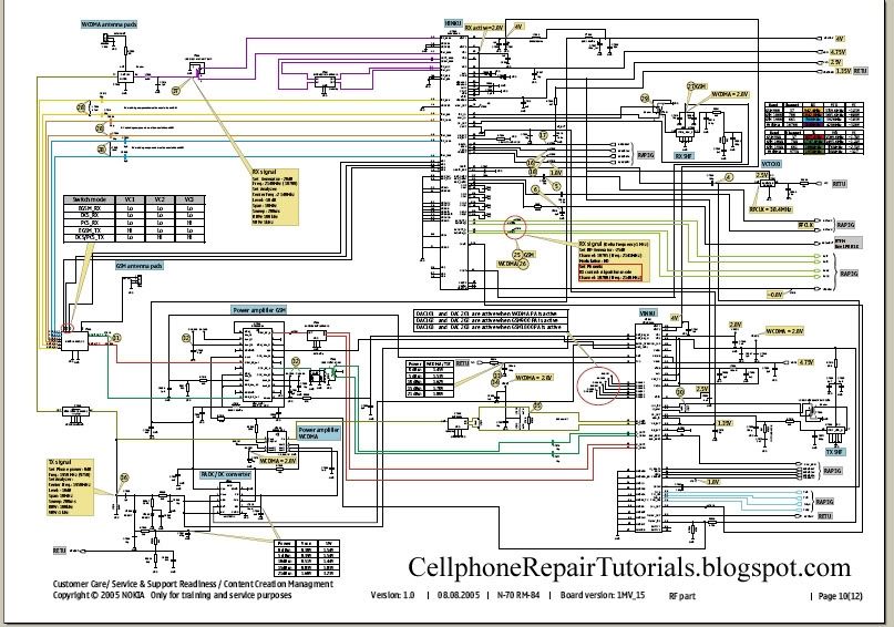
J. page 10, this is the RF components circuit, In this page the
RF or the process of a network during Transmitting and Receiving Radio
Frequency signals.
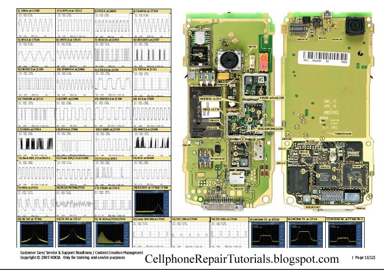
K. page 11, This the structure of the whole PCB Board and all the components mounted in the entire circuit.
this is also where pattern of test-points for check-up during production and servicing.
at the right side is the pattern of waves of frequencies as a guide by using an oscilloscope, frequency generator and spectrum analyzer.
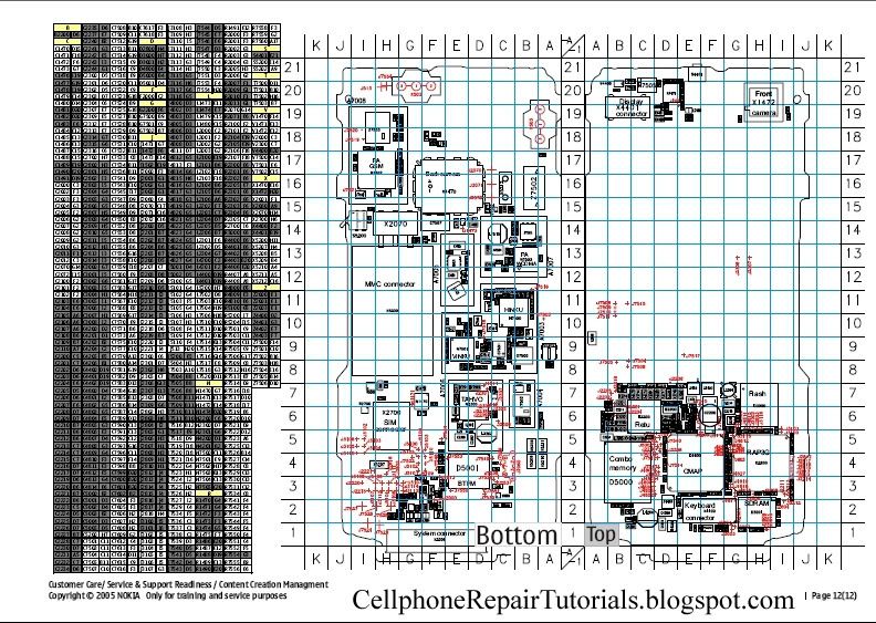
L. page 12, This is where the table of each and every components is mounted on the PCB board written in codes, like Rxxx - resistorr, Cxxx - Capacitor and etc.
The right side is the scale pattern of every components for quick and easy finding it.
that was only the brief explanation of every pages of an Schematic Diagram. Further we will tackle on it even deeper.
Continue reading...
Reading Schematic Diagrams is not a hard task to do, schematic diagrams is a big help to cellphone-repair
especially when working on or tracing lines and finding where a particular components mounted on a PCB board.
Such schematic diagrams is very useful and very important guide in every cellphone technician. It is equivalent to a handbook.
Learn how to read it. At first you might think that it is hard to do so, You are not going to be an experts and master in cellphone repair
as long as you don't know how to read it. Many among cellphone
repairman exist nowadays that do not have any knowledge about reading
it. They always rely on finding free solutions over the internet and
forums. Those people who give free solutions are those people who knows
how to read a schematic diagram.
Now here's your chance to learn and do not rely unto others, and be an
expert and master troubleshooter when it comes to hardware problems.
Okay here's a step on how to read a schematic diagrams.
1. You need to download service Schematic Diagrams, as many or complete package in every cellphone products. each unit of a product have specific service diagrams.
2. You need to download Adobe Acrobat Reader so that you can open the schematic file which is in PDF format.
Now assuming that you already have those I've mention above; Let's try
to open up one file like for example we are going to open a schematic diagram of Nokia N70.
here's what it looks like when scrolling down all the pages.
Let's take a little brief on each page for simple understanding..
A. page 1, In this page where you can find and Identify the whole assembly of the unit.
this is also where to findd the table of contents of the entire circuit's layouts.

B. page 2, In this page is a block diagram of an RF and Baseband:
this is a basic explanation of the entire connection of a circuit. It
was called a block diagram for it is being drawed into blocks.
What is a BASE BAND?
In telecommunications and signal processing, baseband is an adjective
that describes signals and systems whose range of frequencies is
measured from zero to a maximum bandwidth or highest signal frequency;
it is sometimes used as a noun for a band of frequencies starting at
zero. It can often be considered as synonym to lowpass, and antonym to passband, bandpass or radio frequency (RF) signal.
What is a RF?
Radio frequency (RF) is a frequency or rate of oscillation within the
range of about 3 Hz to 300 GHz. This range corresponds to frequency of
alternating current electrical signals used to produce and detect radio
waves. Since most of this range is beyond the vibration rate that most
mechanical systems can respond to, RF usually refers to oscillations in
electronics circuits.

C. page 3, here we can find the system connectors and parts of the unit that correspond to the user or outer parts such us headset, charger and USB connection interfaces.

D. page 4, The power management circuit, audio codecs and drivers and the interfaces like the microphone, earpiece, mouthpiece, vibrator, sim-card, battery connections. This is the Power Supply Area of the entire circuits.

E. page5, Charging Control and Flash Interface Circuit.

F. page 6, This is the part of the circuit where the all application is being process, Flash IC and memories, this also where application and firmware are being stored.

G. page 7, his the Central processing of the unit (CPU) like the personal computer (PC) cellphone also have a CPU to process applications and software.

H. page 8, A Frequency Modulation (FM Radio) circuit.

I. page 9,This page is the part of an LCD Display and Keypad circuit.

J. page 10, this is the RF components circuit, In this page the
RF or the process of a network during Transmitting and Receiving Radio
Frequency signals.

K. page 11, This the structure of the whole PCB Board and all the components mounted in the entire circuit.
this is also where pattern of test-points for check-up during production and servicing.
at the right side is the pattern of waves of frequencies as a guide by using an oscilloscope, frequency generator and spectrum analyzer.

L. page 12, This is where the table of each and every components is mounted on the PCB board written in codes, like Rxxx - resistorr, Cxxx - Capacitor and etc.
The right side is the scale pattern of every components for quick and easy finding it.

that was only the brief explanation of every pages of an Schematic Diagram. Further we will tackle on it even deeper.
With Bass Boost 10W Audio Amplifier High Quality very simple design No preamplifier required
High Quality, very simple design, No preamplifier required
This design is based on the 18 Watt Audio Amplifier, and was developed mainly to satisfy the requests of correspondents unable to locate the TLE2141C chip. It uses the widespread NE5532 Dual IC but, obviously, its power output will be comprised in the 9.5 - 11.5W range, as the supply rails cannot exceed ±18V. As amplifiers of this kind are frequently used to drive small loudspeaker cabinets, the bass frequency range is rather sacrificed. Therefore a bass-boost control was inserted in the feedback loop of the amplifier, in order to overcome this problem without quality losses. The bass lift curve can reach a maximum of +16.4dB @ 50Hz. In any case, even when the bass control is rotated fully counterclockwise, the amplifier frequency response shows a gentle raising curve: +0.8dB @ 400Hz, +4.7dB @ 100Hz and +6dB @ 50Hz (referred to 1KHz).
Amplifier with Bass-Boost:
P1_________________22K Log.Potentiometer (Dual-gang for stereo)
P2________________100K Log.Potentiometer (Dual-gang for stereo)
R1________________820R 1/4W Resistor
R2,R4,R8____________4K7 1/4W Resistors
R3________________500R 1/2W Trimmer Cermet
R5_________________82K 1/4W Resistor
R6,R7______________47K 1/4W Resistors
R9_________________10R 1/2W Resistor
R10__________________R22 4W Resistor (wirewound)
C1,C8_____________470nF 63V Polyester Capacitor
C2,C5_____________100µF 25V Electrolytic Capacitors
C3,C4_____________470µF 25V Electrolytic Capacitors
C6_________________47pF 63V Ceramic or Polystyrene Capacitor
C7_________________10nF 63V Polyester Capacitor
C9________________100nF 63V Polyester Capacitor
D1______________1N4148 75V 150mA Diode
IC1_____________NE5532 Low noise Dual Op-amp
Q1_______________BC547B 45V 100mA NPN Transistor
Q2_______________BC557B 45V 100mA PNP Transistor
Q3_______________TIP42A 60V 6A PNP Transistor
Q4_______________TIP41A 60V 6A NPN Transistor
J1__________________RCA audio input socket
Power Supply :
R11_________________1K5 1/4W Resistor
C10,C11__________4700µF 25V Electrolytic Capacitors
D2________________100V 4A Diode bridge
D3________________5mm. Red LED
T1________________220V Primary, 12 + 12V Secondary 24-30VA Mains transformer
PL1_______________Male Mains plug
SW1_______________SPST Mains switch
Notes:
Output power:
10 Watt RMS into 8 Ohm (1KHz sinewave)
Sensitivity:
115 to 180mV input for 10W output (depending on P2 control position)
Frequency response:
See Comments above
Total harmonic distortion @ 1KHz:
0.1W 0.009% 1W 0.004% 10W 0.005%
Total harmonic distortion @ 100Hz:
0.1W 0.009% 1W 0.007% 10W 0.012%
Total harmonic distortion @ 10KHz:
0.1W 0.056% 1W 0.01% 10W 0.018%
Total harmonic distortion @ 100Hz and full boost:
1W 0.015% 10W 0.03%
Max. bass-boost referred to 1KHz:
400Hz = +5dB; 200Hz = +7.3dB; 100Hz = +12dB; 50Hz = +16.4dB; 30Hz = +13.3dB
Unconditionally stable on capacitive loads
This design is based on the 18 Watt Audio Amplifier, and was developed mainly to satisfy the requests of correspondents unable to locate the TLE2141C chip. It uses the widespread NE5532 Dual IC but, obviously, its power output will be comprised in the 9.5 - 11.5W range, as the supply rails cannot exceed ±18V. As amplifiers of this kind are frequently used to drive small loudspeaker cabinets, the bass frequency range is rather sacrificed. Therefore a bass-boost control was inserted in the feedback loop of the amplifier, in order to overcome this problem without quality losses. The bass lift curve can reach a maximum of +16.4dB @ 50Hz. In any case, even when the bass control is rotated fully counterclockwise, the amplifier frequency response shows a gentle raising curve: +0.8dB @ 400Hz, +4.7dB @ 100Hz and +6dB @ 50Hz (referred to 1KHz).
Amplifier with Bass-Boost:
10W Bass Boost Amplifier Circuit Diagram
Parts:P1_________________22K Log.Potentiometer (Dual-gang for stereo)
P2________________100K Log.Potentiometer (Dual-gang for stereo)
R1________________820R 1/4W Resistor
R2,R4,R8____________4K7 1/4W Resistors
R3________________500R 1/2W Trimmer Cermet
R5_________________82K 1/4W Resistor
R6,R7______________47K 1/4W Resistors
R9_________________10R 1/2W Resistor
R10__________________R22 4W Resistor (wirewound)
C1,C8_____________470nF 63V Polyester Capacitor
C2,C5_____________100µF 25V Electrolytic Capacitors
C3,C4_____________470µF 25V Electrolytic Capacitors
C6_________________47pF 63V Ceramic or Polystyrene Capacitor
C7_________________10nF 63V Polyester Capacitor
C9________________100nF 63V Polyester Capacitor
D1______________1N4148 75V 150mA Diode
IC1_____________NE5532 Low noise Dual Op-amp
Q1_______________BC547B 45V 100mA NPN Transistor
Q2_______________BC557B 45V 100mA PNP Transistor
Q3_______________TIP42A 60V 6A PNP Transistor
Q4_______________TIP41A 60V 6A NPN Transistor
J1__________________RCA audio input socket
Power Supply :

Power Supply Circuit Diagram
Power supply parts:R11_________________1K5 1/4W Resistor
C10,C11__________4700µF 25V Electrolytic Capacitors
D2________________100V 4A Diode bridge
D3________________5mm. Red LED
T1________________220V Primary, 12 + 12V Secondary 24-30VA Mains transformer
PL1_______________Male Mains plug
SW1_______________SPST Mains switch
Notes:
- Can be directly connected to CD players, tuners and tape recorders.
- Schematic shows left channel only, but C3, C4, IC1 and the power supply are common to both channels.
- Numbers in parentheses show IC1 right channel pin connections.
- A log type for P2 will ensure a more linear regulation of bass-boost.
- Do not exceed 18 + 18V supply.
- Q3 and Q4 must be mounted on heatsink.
- D1 must be in thermal contact with Q1.
- Quiescent current (best measured with an Avo-meter in series with Q3 Emitter) is not critical.
- Set the volume control to the minimum and R3 to its minimum resistance.
- Power-on the circuit and adjust R3 to read a current drawing of about 20 to 25mA.
- Wait about 15 minutes, watch if the current is varying and readjust if necessary.
- A correct grounding is very important to eliminate hum and ground loops. Connect to the same point the ground sides of J1, P1, C2, C3 &C4. Connect C9 to the output ground.
- Then connect separately the input and output grounds to the power supply ground.
Output power:
10 Watt RMS into 8 Ohm (1KHz sinewave)
Sensitivity:
115 to 180mV input for 10W output (depending on P2 control position)
Frequency response:
See Comments above
Total harmonic distortion @ 1KHz:
0.1W 0.009% 1W 0.004% 10W 0.005%
Total harmonic distortion @ 100Hz:
0.1W 0.009% 1W 0.007% 10W 0.012%
Total harmonic distortion @ 10KHz:
0.1W 0.056% 1W 0.01% 10W 0.018%
Total harmonic distortion @ 100Hz and full boost:
1W 0.015% 10W 0.03%
Max. bass-boost referred to 1KHz:
400Hz = +5dB; 200Hz = +7.3dB; 100Hz = +12dB; 50Hz = +16.4dB; 30Hz = +13.3dB
Unconditionally stable on capacitive loads
Sonys Camera Fill Light Specific LED Light HVL LE1
Recently, Sony introduced a LED light can be installed in the camera hot shoe, model HVL-LE1. The head can be rotated and comes with light shields, which sell for about $ 250.Is it the 12 volt LED lights.
Sony HVL-LE1 LED light is composed of 60 LED lamps, color temperature has 5500K, the maximum brightness have 1800LUX, you can adjust the sub-file, the minimum output 10%, can be installed in the hot shoe to be used, a filter tank is also designed to be used 3200K filter, the product uses AA batteries or the same rechargeable lithium battery as the Sony A77.
The video below will tell more about this LED Light HVL-LE1.
Continue reading...
Sony HVL-LE1 LED light is composed of 60 LED lamps, color temperature has 5500K, the maximum brightness have 1800LUX, you can adjust the sub-file, the minimum output 10%, can be installed in the hot shoe to be used, a filter tank is also designed to be used 3200K filter, the product uses AA batteries or the same rechargeable lithium battery as the Sony A77.
The video below will tell more about this LED Light HVL-LE1.
Wednesday, June 5, 2013
Electrical Online Content Uploads 2010 Basic Ligh

Loft Lighting Diydoctor Org Uk Diy And Home Improvement Forums.
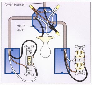
Wiring A 2 Way Switch.

Installing An Additional Light Point 2 Gang Switch.

Light Switch Wiring Diagram Uk Reviews And Photos.

Outlet Switch Wiring1.

Http Www Electrical Online Com Wp Content Uploads 2010 09 Basic Ligh.

Wire Up A Light Switch 4 Wire Up A Light.
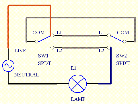
Robots And Projects Two Way Light Switch Wiring.

Trail Lights Page 2 Grizzly Riders Yamaha Grizzly Atv Forum.

Wiring A Light Switch Electrical Online.
Intake Heater Wiring Diagram Questiondodge Dieseldiesel Truck

Personal Plow Plow Gear Parts List And Diagram Item 1 2 3 4 5 6 7 8 9.

Western Snow Plow Unimount Heavy Weight Parts.

Meyer Snowplow Wiring Hoses And Controller Parts And Accessories.

Description 07234 Snow Plow Light Carton More Info 1 07224 Snow Plow.

Intake Heater Wiring Diagram Question Dodge Diesel Diesel Truck.
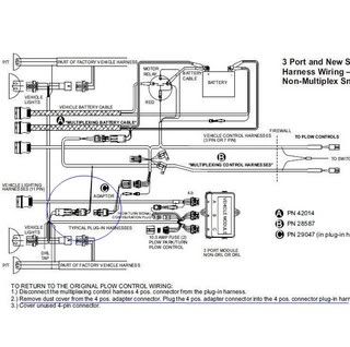
Wiring For Xtreme V Plowsite Com Snow Plowing Ice Management.

Item Part Description 1 61300 6 1 2 Ft Blade Assy Su More Info 2 49264.

Mvp Snowplow Assembly Parts List Hydraulics Box No 66587 Item Part.

Western Snow Plow Wiring Diagrams Group Picture Image By Tag.

Western Ultramount Flostat Hydraulic Unit Breakdown Plow Parts.
Labels:
diagram,
dieseldiesel,
heater,
intake,
questiondodge,
truck,
wiring
Electric Flux Distribution Schematic Diagramcircuit Schematic

Over 800 Fender Guitar Amps Wiring Schematics Manuals For Sale.
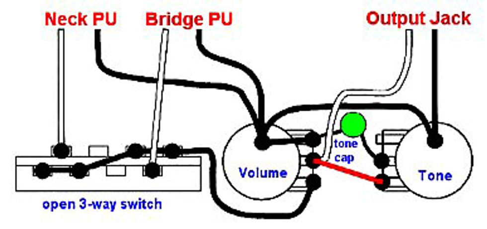
Fender Wiring As Well As The 50s Gibson Vintage Wiring.

Eddie Van Halen S Frankenstrat Pictured With 22 Fret Kramer Neck.

Notes The Pots R1 R3 Are All Audio Taper They May Be Either 500k Or.

The Following Guitar Wiring Diagram Book Contains Artec Wiring.

281 Permalink Re Wiring Library Or Is This One Better.

Electric Flux Distribution Schematic Diagram Circuit Schematic.
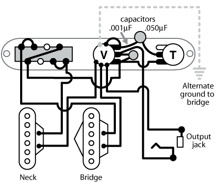
Explain 52 Tele Reissue Selector Switch Telecaster Guitar Forum.

Diagram Nokia 5530 Board Related Posts Nokia N97 Exploded View Diagram.

Kathryn Erbe Photos Ford Ignition Wiring Diagram.
Labels:
diagramcircuit,
distribution,
electric,
flux,
schematic
Subscribe to:
Comments (Atom)